There are a few HOWTOs for this method. However not very
detailed, and I had to find out a couple of things by myself.
So this is my version. THT, as well as SMD (less effort) is
possible. Until now I've only produced one-layer-PCBs.
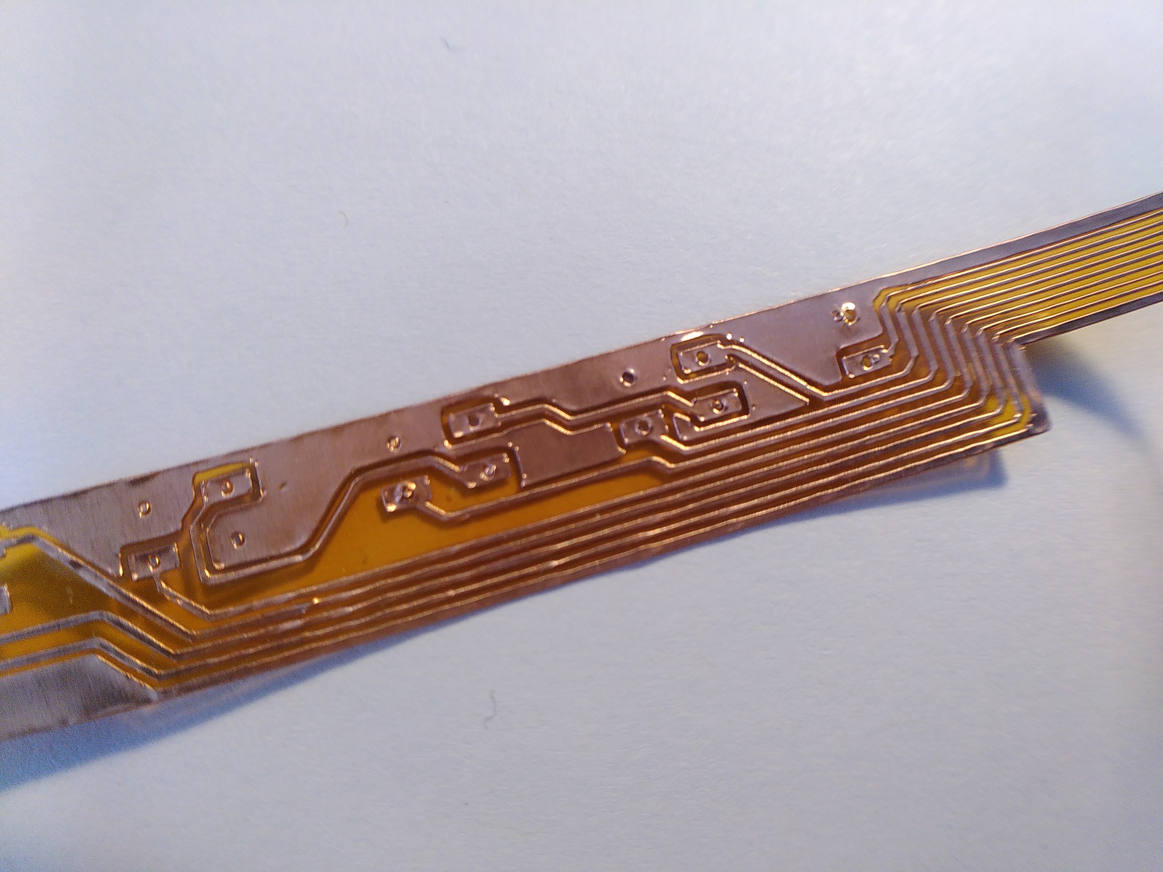
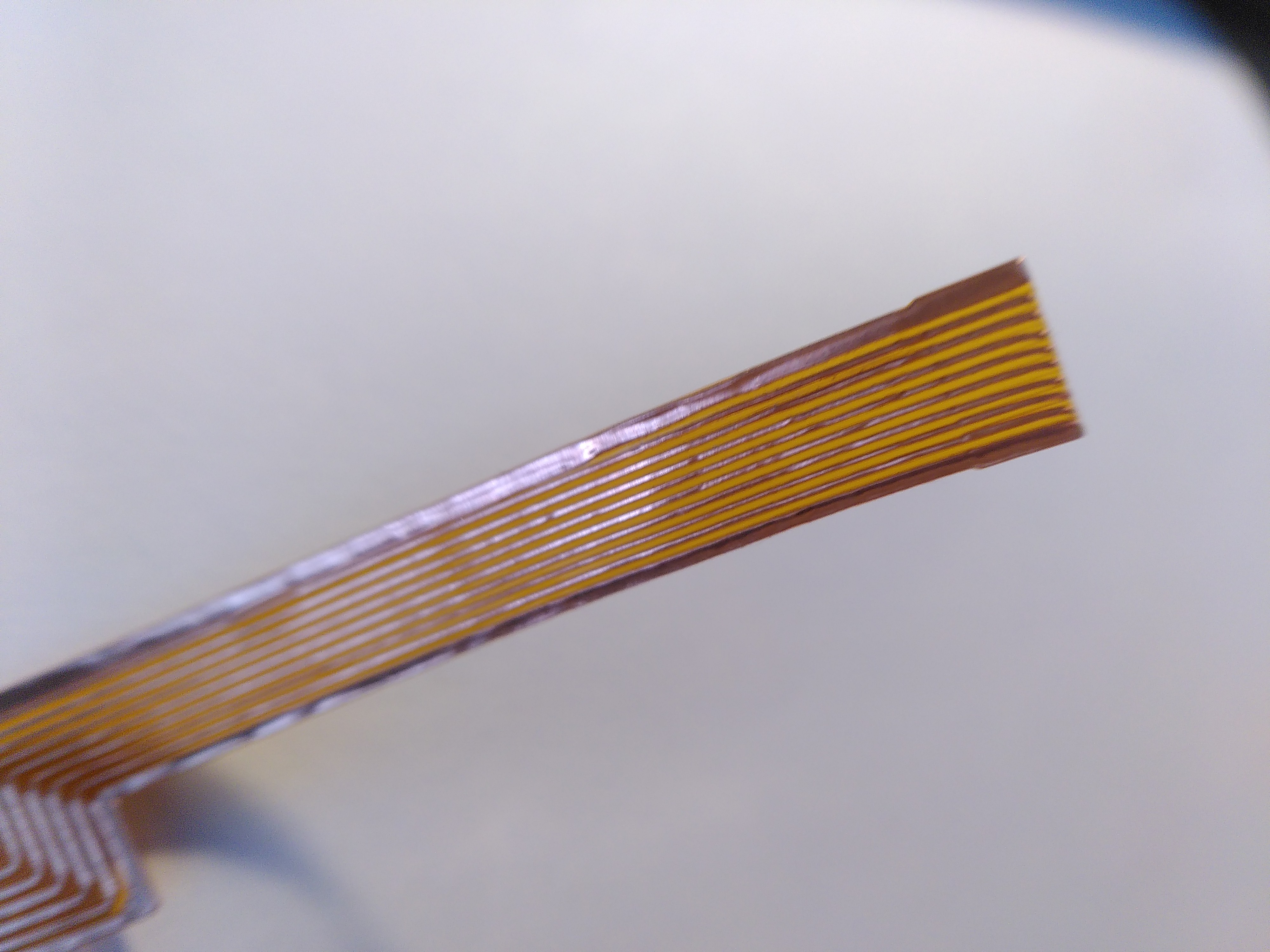
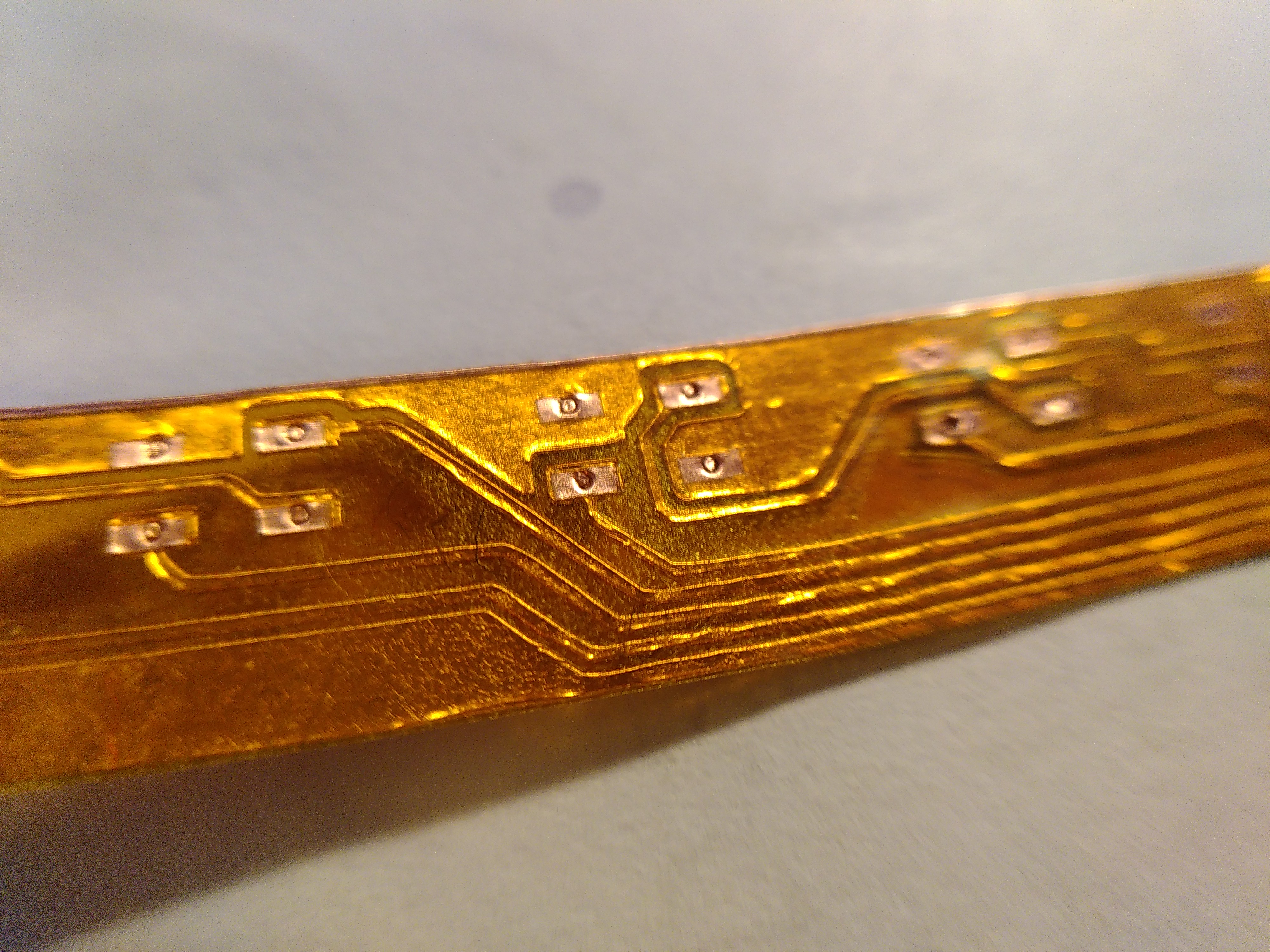
update: Flexible PCBs (more docs follow)
0,4mm / 0,5mm trace width
With soldermask:
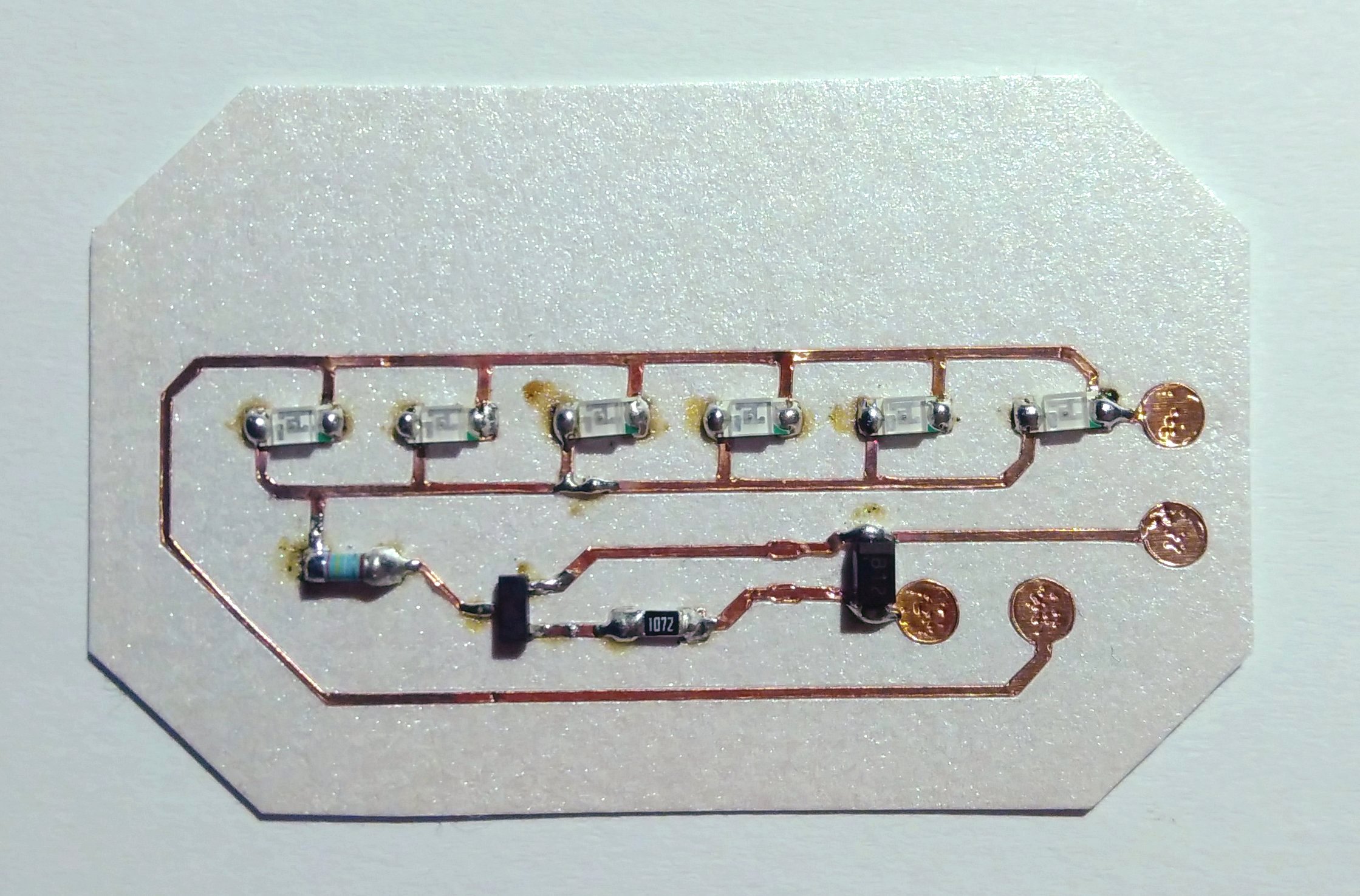
This is how a populated PCB from a cutting plotter can look like.
Trace-width is 0.6mm:
Required materials:
-cutting plotter
-in my case a 2nd-hand "Silhouette Portrait 2"
with "autoblade"-knife. But there aren't any special requirements
for the type of cutting-plotter
-standard cutting mat,slightly sticky
-self-adhesive copper foil
-I've used "guitar pickung foil". My first one
was significantly thicker than the one, which is shown in this
example:
"Guitar pickup copper foil 300 x 200mm Self
Adhesive". Small pieces are enough, Minimum dimensions a bit more,
than the PCB than you want to be plotted
-the exact thickness of the copper foil is
unknown, but I guess more than the typical values for the cupper
layer on common PCBs
-Substrate cardboard
-not too rough: Otherwise you can't peel of the
cut-out parts, without breakaway the cardboard
-glossy but not too glossy: Otherwise the parts
that should stick, won't stick enough
-best material so far:
Glossy paper for self-made gift cards
-to find
out which substrate is suitable, you can just glue a little
piece of copper foil onto it:
It should stick good enough, but when you peel it of, there mustn't
breakaway scraps of paper with it
Required software:
-PCB-design software
-tested with KiCad (open-source). All
layout-programs should make it, as far as they can export dxf
-software for cutting-plotter
-vendor software for Silhouette Portrait 2, free
with a few restrictions that don't matter
-runs also in Linux with
VirtualBox
-alternative: Plugin for InkScape - I couldn't
make all settings make what they should do: https://github.com/fablabnbg/inkscape-silhouette
HOWTO:
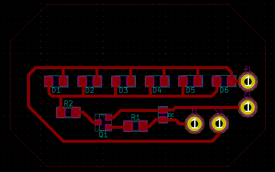
1. Example-layout, made with
KiCad, mostly SMD, four pin-holes for wires.
The edge-cut is set to the upper copper layer:
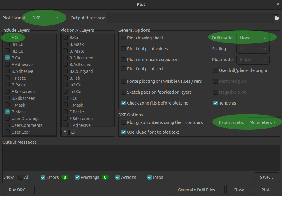
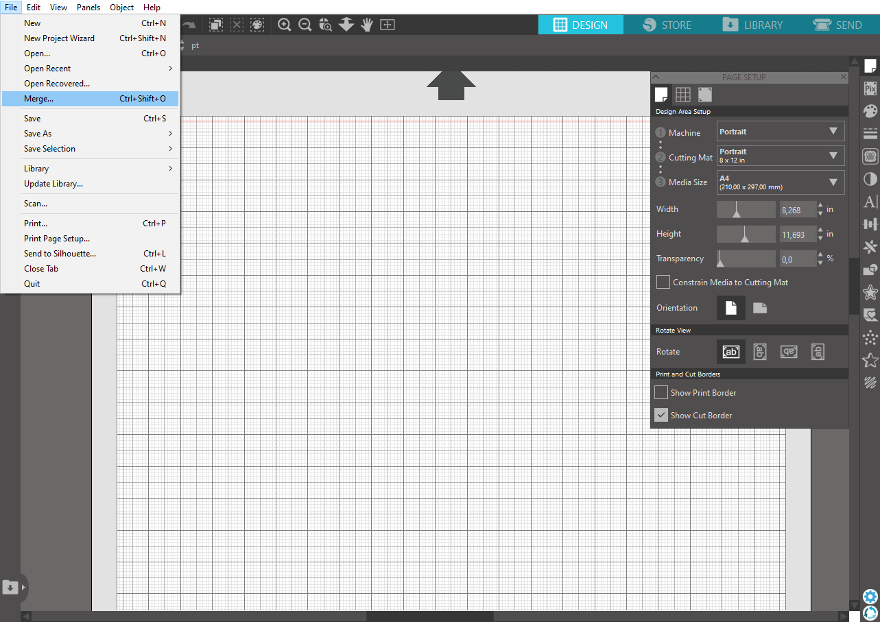
2. In KiCAD menu select "File /
Merge..." and maybe change settings.
The units must be the same
as later in the plotter-software:
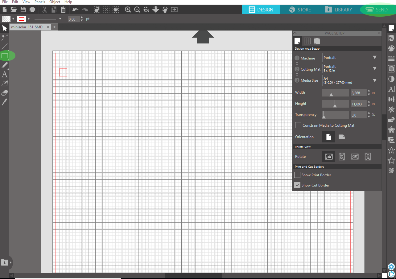
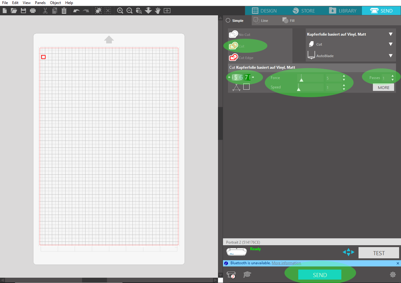
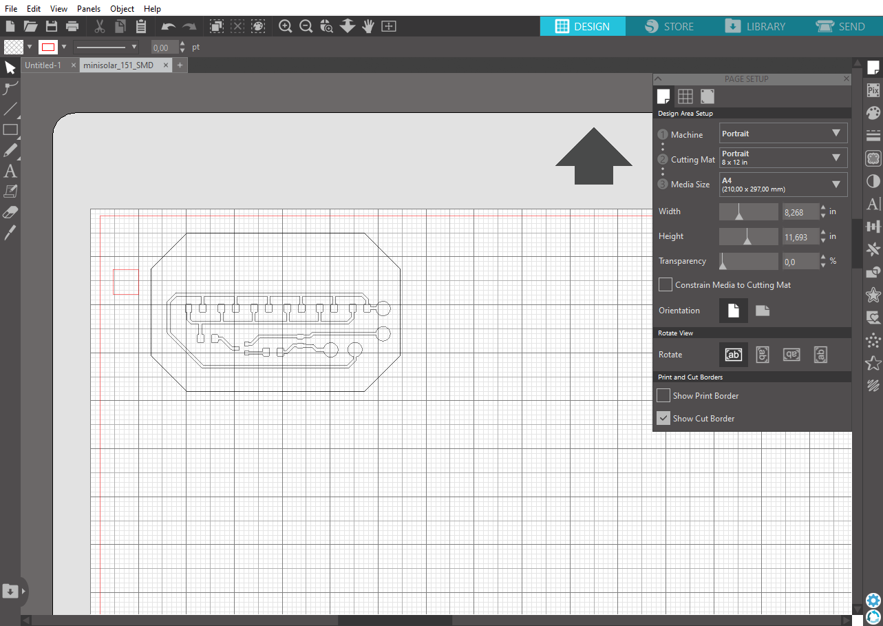
3. In Silhouette Studio select the machine
and cutting mat, if this isn't already default.
Optional: I suggest drawing a little sqaure, to find out the best
settings for plotting:
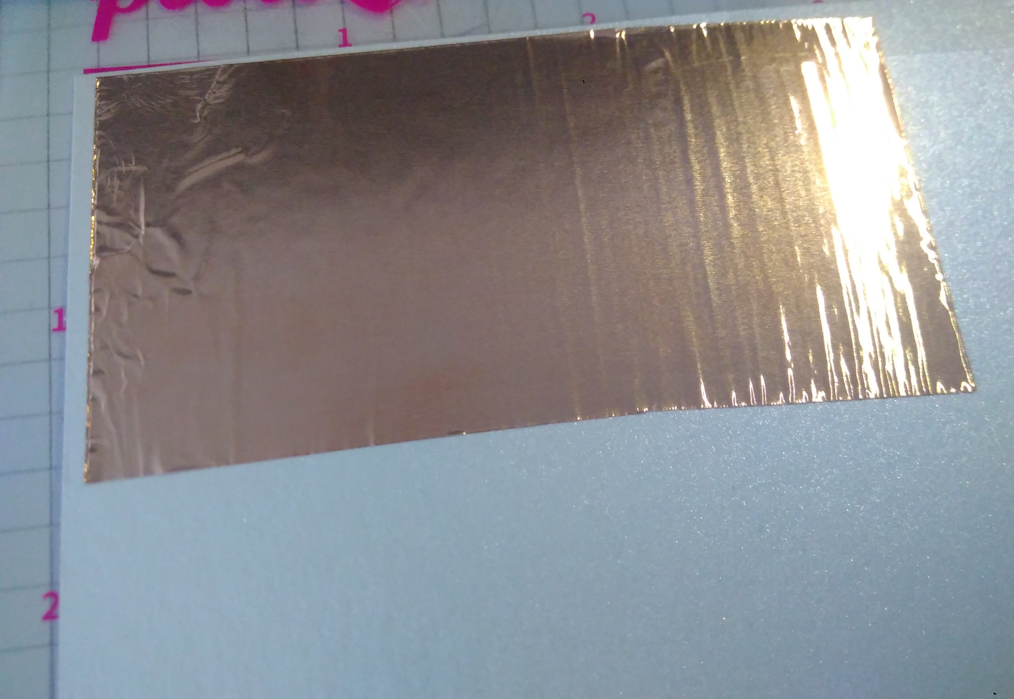
4. Now peel of the protection shielt. and
glue the copper foil onto the glossy paper. After that glue both
together onto a lightly adhesive cutting mat:
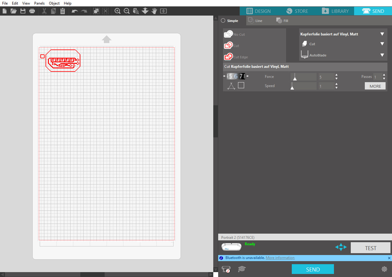
5. By clicking "send" there comes a new view
with the settings for cutting depth, force and speed.
Put the cutting mat with glued
on copper-foil-cardboard into the plotter and press "send".
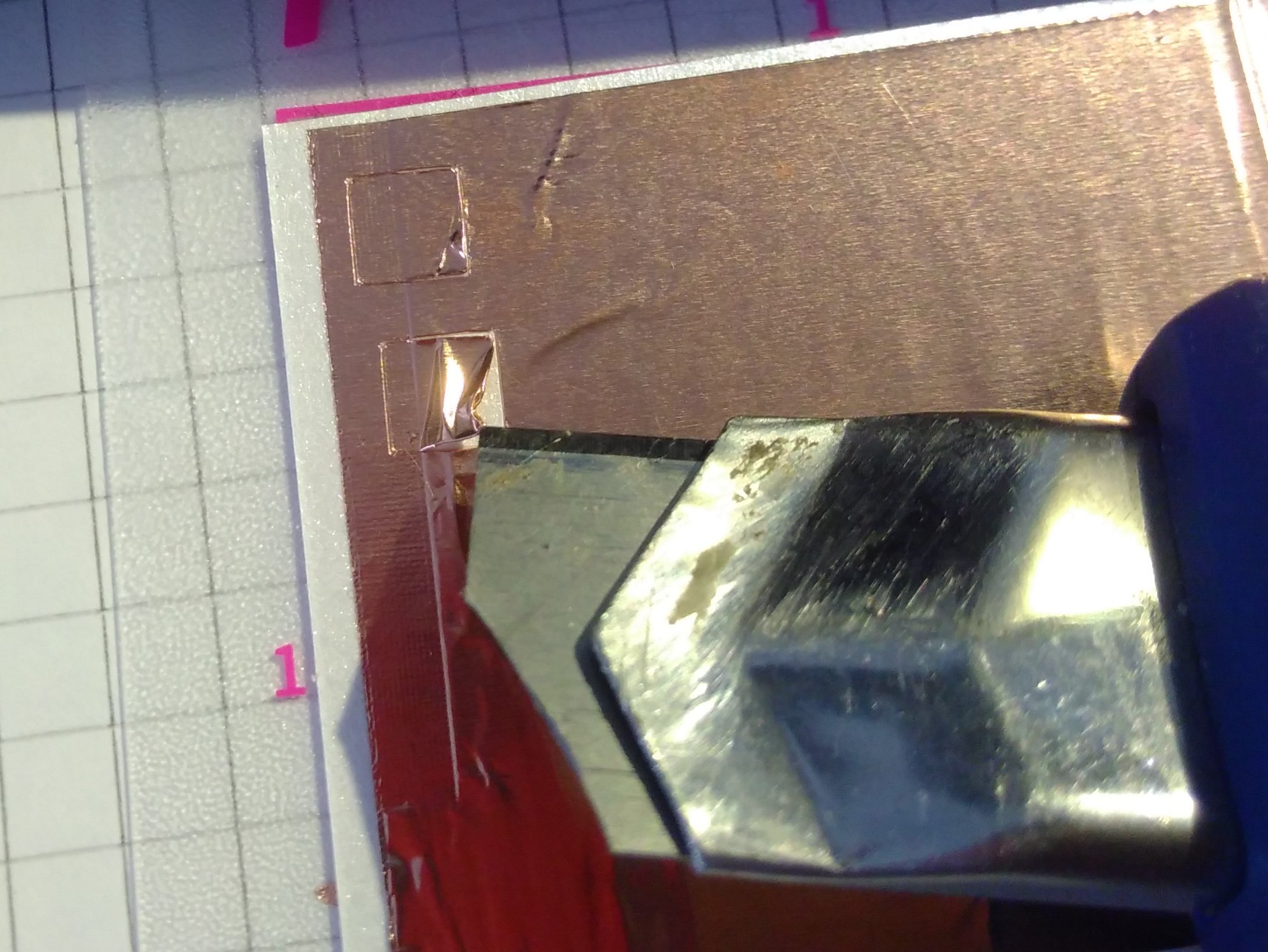
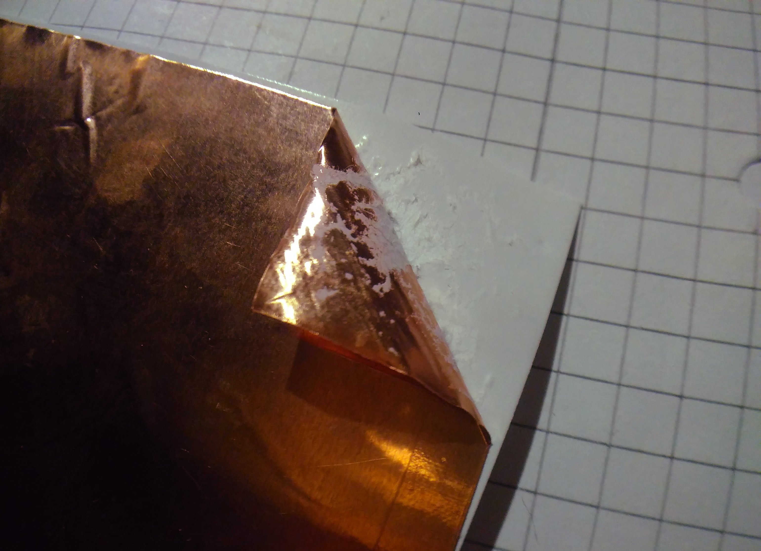
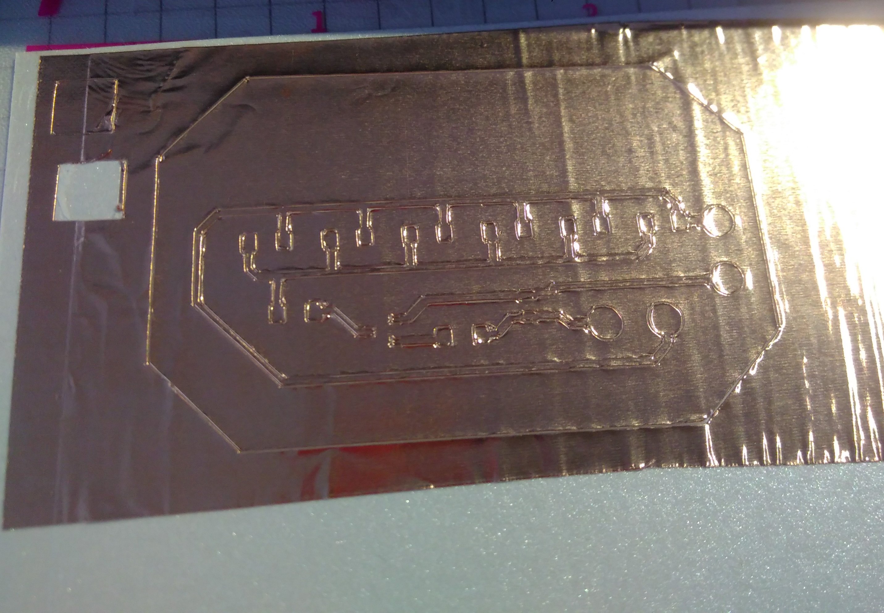
6. The foil should peel of pretty easy, and
the copper foil around it must not rip paper with it:
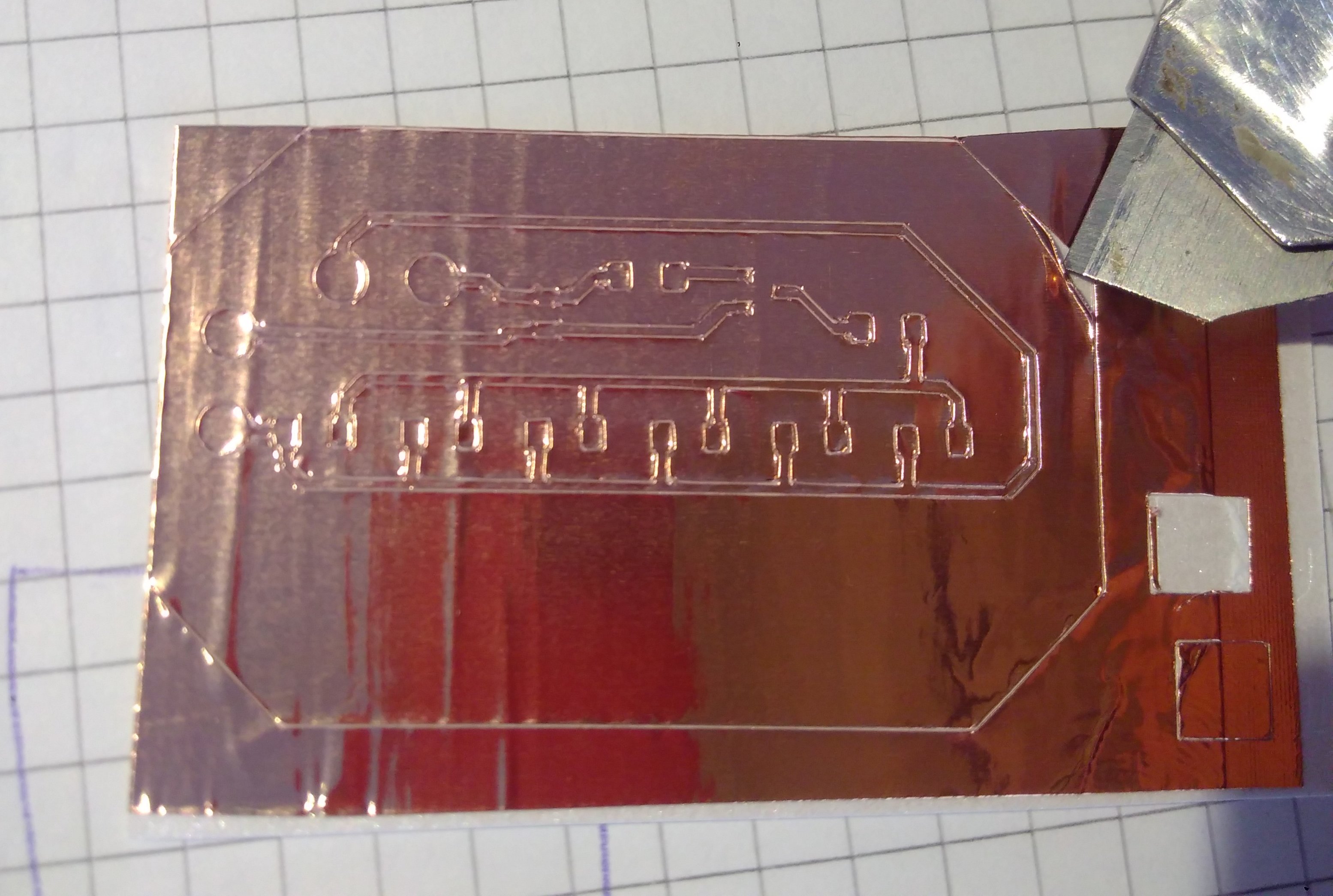
This is an faulty example, the glue rips of the paper:
7. Now switch to "design" and merge the
PCB-layout:
8. Then plot the PCB just like the little
square before. The square can also be deleted:
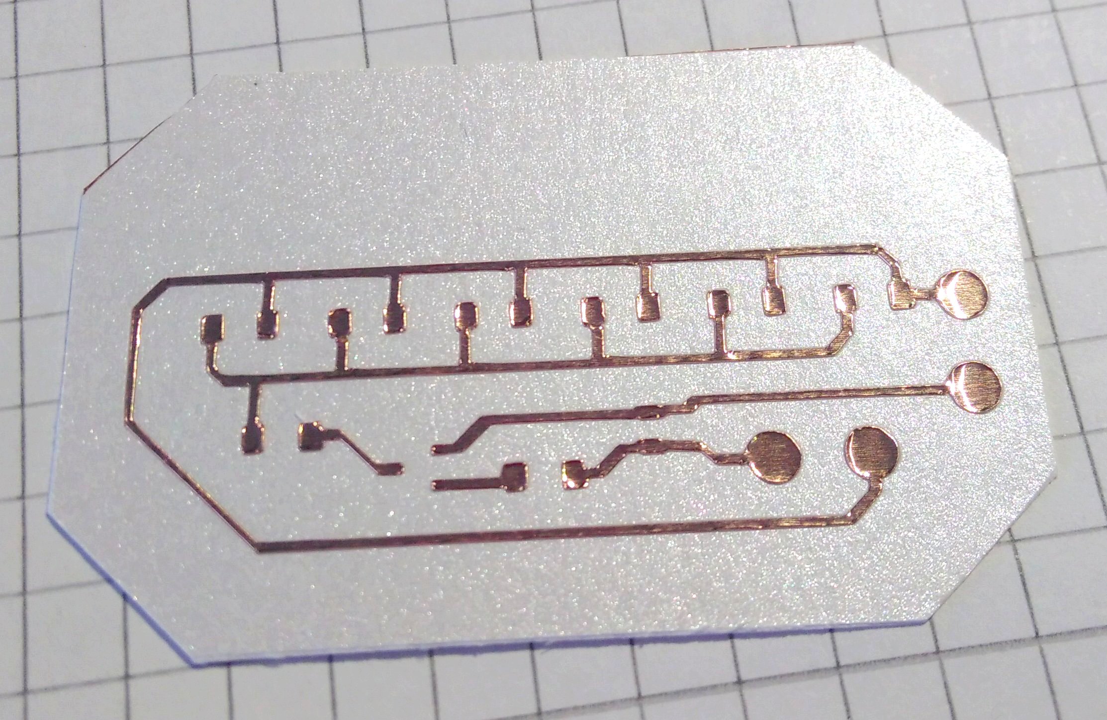
9. The result:
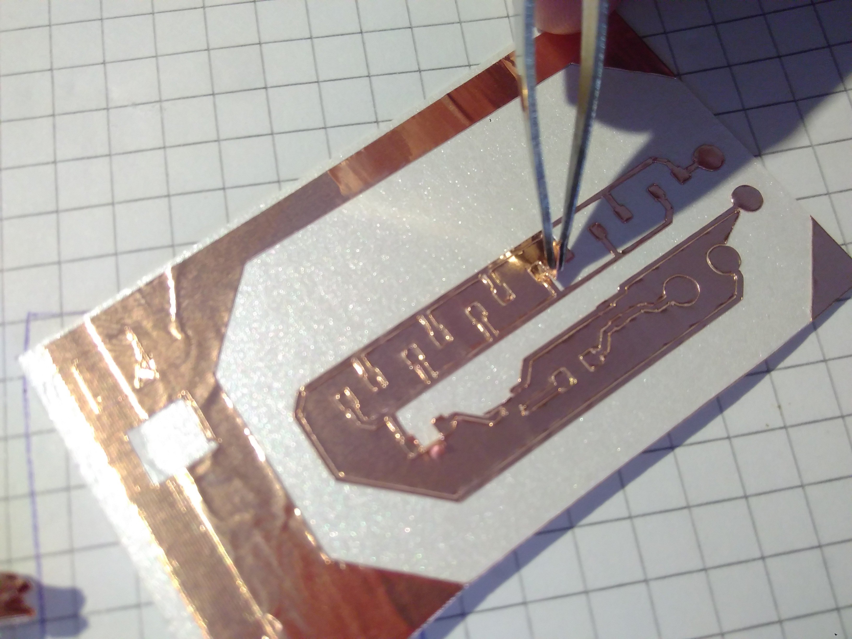
10. Now peel of the foil around the traces.
Cut out the PCB with scissors...
 Licensed under Creative
Commons Attribution-NonCommercial-ShareAlike 4.0 International
License.
Licensed under Creative
Commons Attribution-NonCommercial-ShareAlike 4.0 International
License.